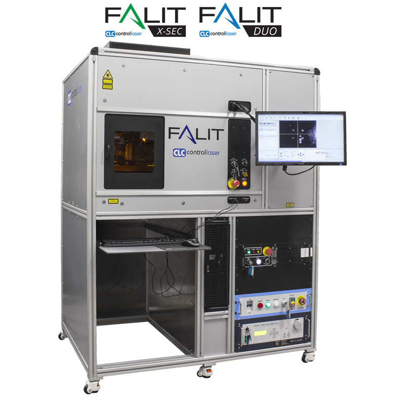
Our FALIT™ (pronounced “F-A-Light”) was specifically designed with the Semiconductor Failure Analysis Lab in mind. The FALIT™ incorporates a patented laser decapsulation process with multiple laser configurations and wavelengths to provide clear and precise test samples for every type of semiconductor failure analysis application. The FALIT™ allows a faster and more accurate method for Failure Analysis semiconductor processing. Our patented semiconductor laser decapsulation ablation technology provides clean, accurate laser decapsulation, and more.
- Ideal Solution for IC Laser Decapsulation, Gel Removal, Cross-Sectioning, and Delidding Components.
- Cleanly remove mold compound using laser technology rather than the traditional unsafe Acid process.
- Expose Wire Bonds without Damage to other components.
- Air-cooled (except for the optional UV laser).
- Integrated safety shutter to avoid potential beam exposure.
- FALIT™ Laser Software interface included. Fully featured, GUI for Failure Analysis.
The FALIT™ systems provide Laser Decapsulation (ablation) and Laser Cross-sectioning of semiconductors for failure analysis labs. CLC IC laser decapsulation systems are used in many semiconductor failure analysis labs to remove mold compound, de-lid semiconductor hermetically-sealed cases, remove various gels, and cross-section ICs for further inspection. Our patented process has been refined over the 10-plus years since it’s existence.
For laser decapsulation, you will want to look at our latest technology, the Digital ICO™ laser.
This specialized laser source is the key to uncovering mold compound all the way to the die in some cases. Digital ICO™: Gets you closer. The FALIT™ can import images from a variety of test imaging process Such C-SAM, SEM, SAM and even X-RAY to show the exact location Where ablation of the EMC is required for further forensic processing.
ALL FALIT™ systems are certified as CLASS 1 product in accordance with Title 21, Code of the Federal Regulations, sub-chapter J, (21 CFR), and the European standard EN 60825:1992

USA: 7,271,012 B2
JAPAN: 4,843,488
CHINA: ZL200480022971.0
PHILIPPINES: 1-2006-500131
EUROPE: 04778639.7
CANADA: 2,532,959
KOREA: 10-2006-7000841


